Frequently Asked Questions
PCB Assembly and Electronic Manufacturing: Frequently Asked Questions
Detailed answers to the questions hardware teams ask most about quoting, files, pricing, sourcing, quality and delivery.
Last updated: September 2026
This page answers the questions hardware teams ask most often about PCB assembly (PCBA), electronic component sourcing and turnkey manufacturing. Everything here reflects the current production capabilities and working model of SMT Labs, an Istanbul-based EMS company; prices are quotes, set by quantity and technical requirement.
PCB Assembly and Fabrication
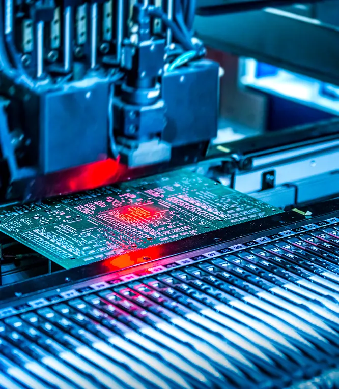
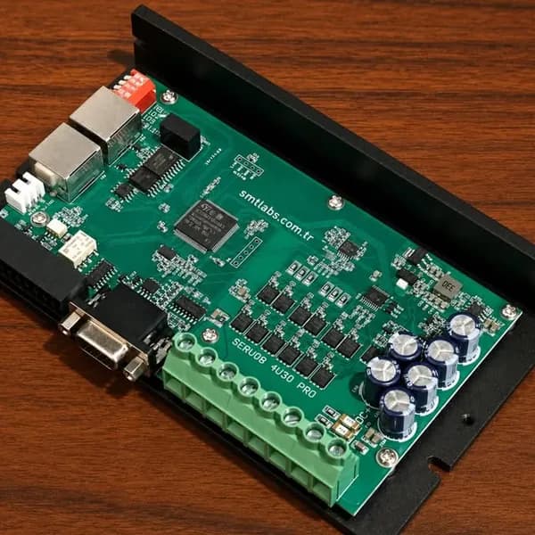
PCB assembly (PCBA, Printed Circuit Board Assembly) is the placement and soldering of electronic components onto a printed circuit board using surface-mount (SMD) and through-hole (THT) methods. The result is a board with its components mounted, ready to work.
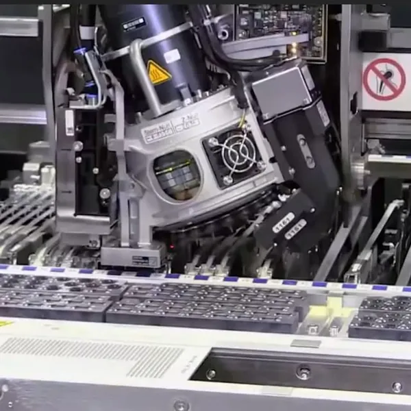
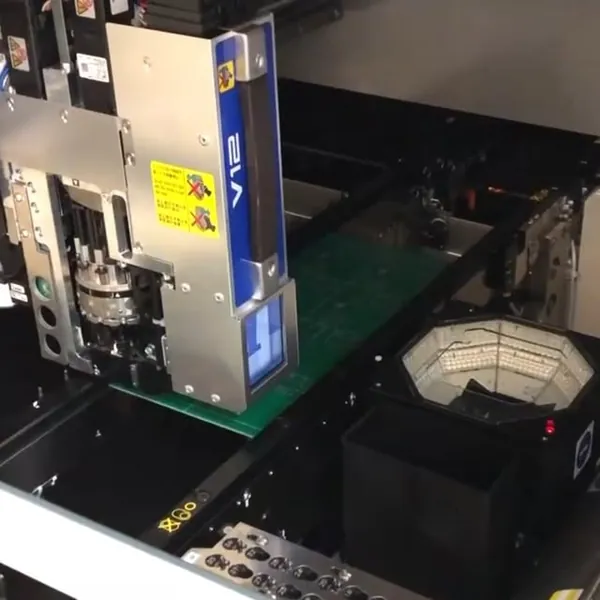
At the facility in Maslak, Istanbul, SMT Labs runs an automated line from prototype to volume production. The flow is solder-paste printing, SPI, high-speed pick & place, multi-zone reflow soldering and post-placement AOI.
- SMD: from 0201 and 01005 packages to QFN, QFP and BGA/µBGA
- THT: connectors, relays, power parts; selective and hand soldering
- Single and double-sided boards in one flow
In SMD (surface-mount) assembly, components are placed on the board surface and soldered in a reflow oven; it is ideal for small packages, high density and automation. In THT (through-hole) assembly, component leads pass through holes in the board and are soldered; it is preferred for mechanically loaded connectors, relays and power parts.
Most modern boards are mixed. SMT Labs combines SMD and THT on the same board in a single order, with THT supported by selective and hand-solder stations.
Our placement range runs from the 0201 package to BGA and µBGA. Very small passives such as 01005, and fine-pitch parts such as QFN, QFP and LGA, are placed as standard.
Solder quality under hidden-connection parts such as BGA and µBGA is checked by X-ray; a reball is applied where needed.
Yes. We work across every volume range, from a single prototype to low-volume series and high-volume production. The target lead time for sample boards is about 10 business days.
Prototype and series run on the same line with the same parameters, so a design proven in the prototype moves to series production without surprises.
We supply printed circuit boards from one to 64 layers. Materials include standard FR4, high-Tg FR4, aluminium-backed (MCPCB) for heat dissipation, and flex / rigid-flex for bendable applications.
Surface finishes include HASL, lead-free HASL, ENIG and HDI. When you combine PCB fabrication with assembly and component sourcing, a single Gerber + BOM submission returns an assembled board.
Pricing and Quotes
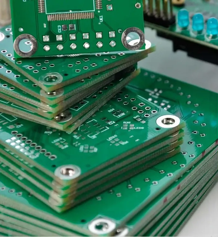
The assembly price is not set from a fixed list but calculated with project-specific parameters. Once you send your Gerber, BOM and Pick & Place files, we return an exact price and lead time within 24 hours.
The main factors that drive the price:
- Board quantity (unit cost drops sharply in series production)
- Component count and variety (many different packages mean more feeder changes and setup time)
- SMD / THT ratio, fine pitch and BGA density
- Single or double sided, stencil need
- Leaded / lead-free solder profile
- Extra quality control such as AOI, X-ray, ICT or functional test
Yes. If you consign the components, the quote covers only the assembly labour and any stencil / setup fee; no material cost is added. If you hand us the BOM, we take on sourcing original parts from three continents and the material cost is included in the quote.
A mixed model is also possible: you send the critical parts, we source the rest.
The fastest route is to send the Gerber + BOM + Pick & Place files and the target quantity. If you have no design files yet, we can give an indicative price from clear photos of the existing board, an approximate component count and the quantity.
Files and the Ordering Process
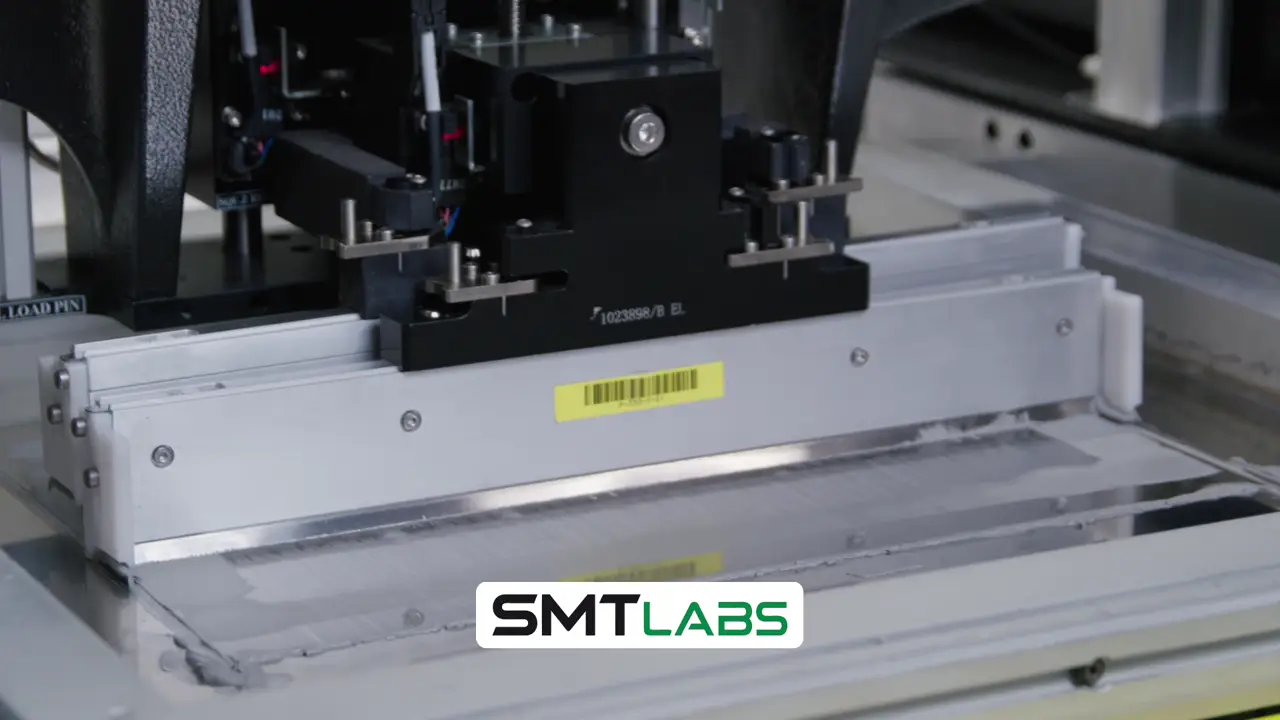
Three files are enough: Gerber for board fabrication and stencil, an LCSC-compatible BOM for the component list, and a Pick & Place (CPL) file for placement coordinates.
Including a fab drawing in the Gerber package, and providing stackup, impedance requirement and quality class (Class 2/3), speeds up the quote.
If files are missing, we derive what we can from the existing board and report the gaps with DFM notes. If there is no Pick & Place, coordinates can be derived from the Gerber and BOM; in that case an extra verification step is added.
The process runs in four steps:
- 1. Send the files: Gerber, BOM and Pick & Place (or a photo of the existing board and the quantity).
- 2. Quote in 24 hours: DFM notes, price and lead time.
- 3. Approval and sourcing: PCB, stencil and component supply; an approved alternative for out-of-stock parts.
- 4. Production and shipping: assembly, AOI and testing are completed; boards ship from the Istanbul central warehouse across Turkey.
Yes. We start the conversation with whatever documentation you have. If the design is incomplete, the engineering support team clarifies the gaps (component selection, footprint, DFM), then we move to production. If you prefer, we run PCB, components, assembly, firmware loading and test as a single turnkey project.
Component Sourcing and Import
Yes. When you send the BOM, we source every part from original suppliers through a network across three continents. Each BOM line is priced by MPN and quantity; stock, lead time and price come back in one table.
Import, customs clearance, origin and conformity paperwork run on the SMT Labs side, so long and variable customs processes leave your agenda. The quote shows part cost, freight, customs and related taxes as separate, transparent line items.
Quality, Test and Certification
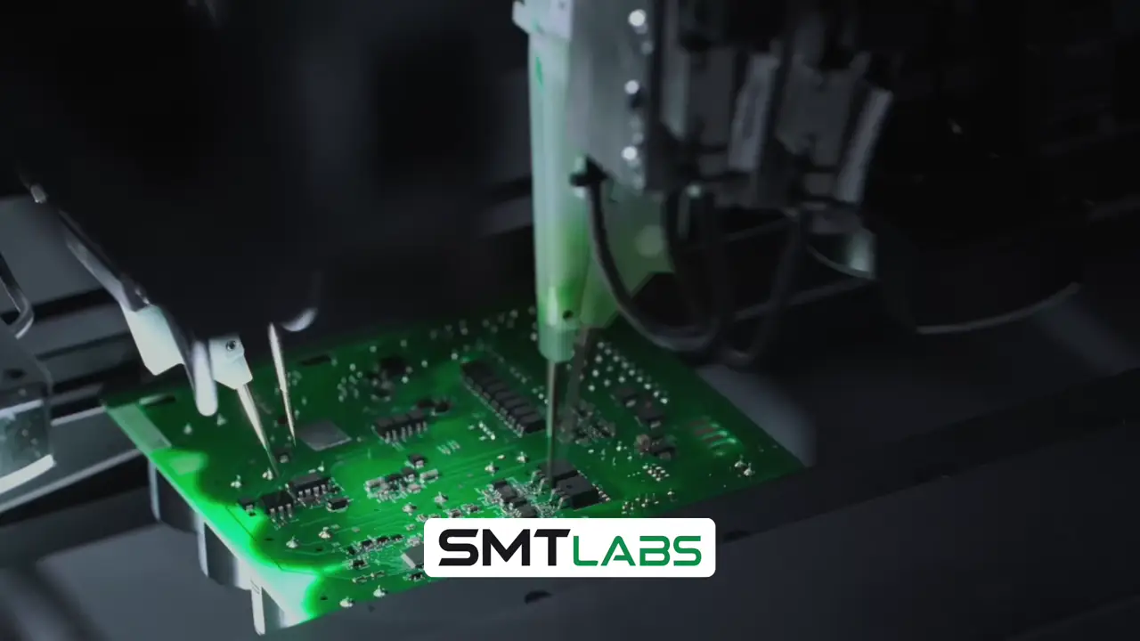
Quality control is built into the production flow. Post-print SPI (solder-paste inspection) and post-placement AOI (automated optical inspection) are standard; X-ray for connections under BGA/µBGA, and ICT and functional test for electrical verification, are offered as options.
- SPI: paste volume and alignment
- AOI: placement, polarity, solder quality
- X-ray: solder under BGA/µBGA
- ICT / functional test: electrical and functional verification
Production follows the IPC-A-610 Class 2 and Class 3 acceptance criteria. The class is chosen by the board's application: Class 2 for general industrial products, Class 3 for uses where uninterrupted performance is critical (defence, aerospace, medical).
Connections under hidden-connection parts such as BGA and µBGA are imaged by X-ray; voids, bridging and open circuits are caught this way. If a fault is found, a reball is applied and the result is re-verified by X-ray.
Our quality management approach aligns with ISO 9001, environment with ISO 14001, occupational health with ISO 45001 and information security with ISO 27001; material compliance follows RoHS and REACH. Accredited certificates will be added to the quality policy page as they are issued.
Delivery and Logistics
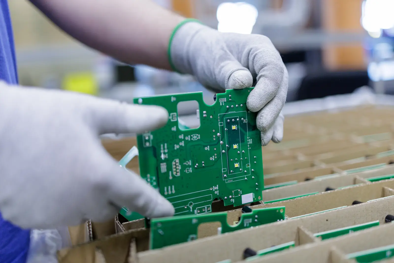
Yes. Production takes place at the facility in Maslak, Istanbul; boards are packed and shipped anywhere in Turkey with the courier you choose. Sample and series deliveries are managed from one address.
Consolidation, import and customs clearance of parts bought from overseas suppliers are within our logistics service. Parts from different sources are merged at one point and sent as a single shipment, so lead time and cost stay predictable.
Working Model and Company

In piece-by-piece (partial) service you coordinate PCB, components, assembly and box-build. In turnkey, SMT Labs takes on that coordination, the fit risk and single-lead-time delivery; PCB fabrication, component sourcing, SMD/THT assembly, firmware loading, functional test and box-build are brought into one project plan.
We work where reliability and precision are critical: defence, aerospace, automotive and transport, communication technologies, robotics and automation, energy and power electronics, medical and consumer electronics.
Yes. We run contract electronics manufacturing (EMS) agreements with repeatable processes. The sample batch is simplified with DFM feedback, the approved design moves to series with the same parameters, and revisions are tracked with a version record.
SMT Labs operates within SMT Global Mühendislik A.Ş. in Maslak, Istanbul (Giz 2000 Plaza). Our team has more than 15 years of hands-on experience in electronic manufacturing and import; that experience shows up as the right DFM and process decisions, and production that is right the first time.
For a quote, upload your Gerber, BOM and Pick & Place files through the form on our contact page; price and lead time come back within 24 hours. Phone, email and WhatsApp details are on the same page.
Related pages
Quote
Ready to start your PCB assembly with next-generation equipment?
Send your Gerber and BOM files and we'll get back to you quickly with pricing and lead time.
For a PCB assembly quote
- 01PCB layout Gerber file.zip
- 02LCSC-compatible BOM list.csv / .xlsx
- 03JLCPCB-compatible Pick & Place file.csv / .cpl
Sample file formats
- gerber-ornek.zip
- bom-ornek.xlsx
- pick-and-place-ornek.csv
Sample templates coming soon.