
Legal
Distance Sales Agreement and Pre-Information Form
The sales terms that apply to PCB, PCBA and component orders placed through the website or the order tracking system.
Last updated: September 2026
Parties
Seller: SMT Global Mühendislik İthalat İhracat Sanayi Ticaret A.Ş. (the "Company"). Address: Maslak Mah. Eski Büyükdere Cad. Giz 2000 Plaza No: 7 İç Kapı No: 34, 34485 Sarıyer / İstanbul. Email: info@smtlabs.com.tr · Phone: +90 212 909 18 56.
Buyer: the individual or legal entity who places an order electronically through the Company's website or order tracking system and approves this agreement.
Subject
This agreement governs the parties' rights and obligations regarding the sale, production and delivery of custom-made PCB (bare board), PCBA (assembly) and electronic component sourcing products/services requested by the Buyer by submitting a Gerber file, schematic and/or bill of materials (BOM), under Turkish Consumer Protection Law No. 6502 and the Distance Contracts Regulation.
Nature of the product and production process
- PCB (bare board): the Gerber files submitted by the Buyer are forwarded by the Company to our production partner JLCPCB for fabrication. The Company acts as a supplier/intermediary at this stage.
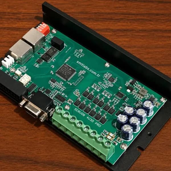
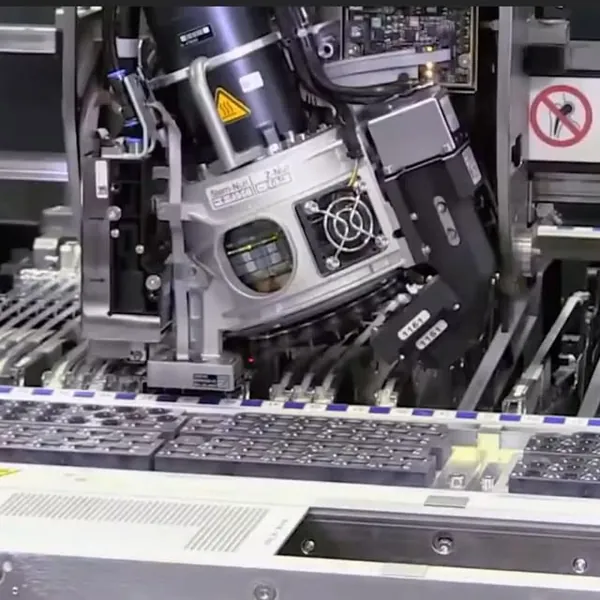
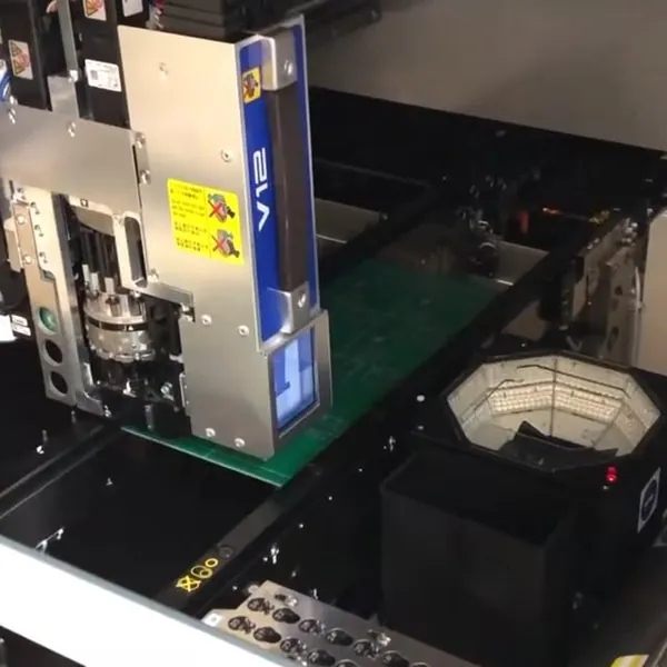
- PCBA (assembly): placement and soldering of SMD and THT components is carried out on the Company's own production line in Maslak, Istanbul, to IPC-A-610 Class 2/3 standard with AOI/ICT quality control.
- Electronic component sourcing: components requested by the Buyer are sourced by the Company from domestic and international suppliers.
Right-of-withdrawal exception
Under Article 15/1-b of the Distance Contracts Regulation, the right of withdrawal does not apply to "contracts for goods prepared according to the consumer's requests or personal needs." PCB and PCBA products manufactured according to the Buyer's submitted Gerber file, schematic or specific requirements are entirely custom-made for that person/company. Accordingly, the Buyer has no right of withdrawal once the order is confirmed and production has started.
Delivery and lead time
Lead time varies by order; it is stated as an estimate in the quote or proforma invoice based on order quantity, board complexity, PCB sourcing time and customs/logistics processes. No single fixed lead time is promised for all orders.
Because PCB sourcing depends on an international production and shipping process, reasonable delays may occur at that stage. The PCBA (assembly) stage is run on the Company's own line and is therefore directly within the Company's control.
Liability
PCB fabrication: the Company is responsible to the extent that it forwards the Buyer's design files to JLCPCB and follows up on the order. For defects arising directly from JLCPCB's manufacturing process (tolerance deviation, material defect, etc.), the Company will pursue a resolution on the Buyer's behalf through JLCPCB's own quality/warranty process, but cannot be held directly liable for such fabrication-caused defects.
PCBA (assembly): since this stage is carried out on the Company's own production line and quality-control process, any defect confirmed to originate from assembly (e.g. missing/faulty soldering, incorrect component placement) is assessed by the Company and resolved on a case-by-case basis (rework, partial refund, etc.).
Force majeure
Official/local holidays in the manufacturing country, changes in or holds under customs regulations, international shipping disruptions, natural disasters, epidemics, war and similar extraordinary circumstances affecting the PCB sourcing process are considered force majeure. Extraordinary events affecting the Company's own production line, such as fire or natural disaster, are treated the same way. In the event of force majeure, the parties will notify each other within a reasonable time.
Electronic approval and effective date
This agreement takes effect, with the same legal force as a wet-signed contract, at the moment the Buyer ticks the relevant approval checkbox electronically when completing an order.
This text is for information only. The binding final version must be reviewed by your legal counsel before it takes effect. Details shown in square brackets will be updated once registration and setup are complete.
Расчёт
Готовы начать монтаж плат на оборудовании нового поколения?
Отправьте файлы Gerber и BOM, и мы быстро вернёмся к вам с ценой и сроком.
Для расчёта монтажа плат
- 01Файл Gerber с топологией платы.zip
- 02Список BOM, совместимый с LCSC.csv / .xlsx
- 03Файл Pick & Place, совместимый с JLCPCB.csv / .cpl
Примеры форматов файлов
- gerber-ornek.zip
- bom-ornek.xlsx
- pick-and-place-ornek.csv
Примеры шаблонов скоро.